Printed Circuit Board

IATF16949 / ISO9001 /ISO14001/ISO13485/GBT29490
Cetified
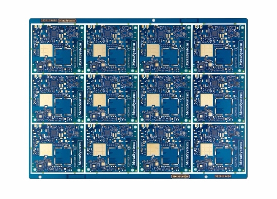
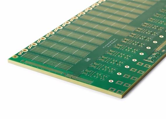
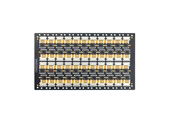
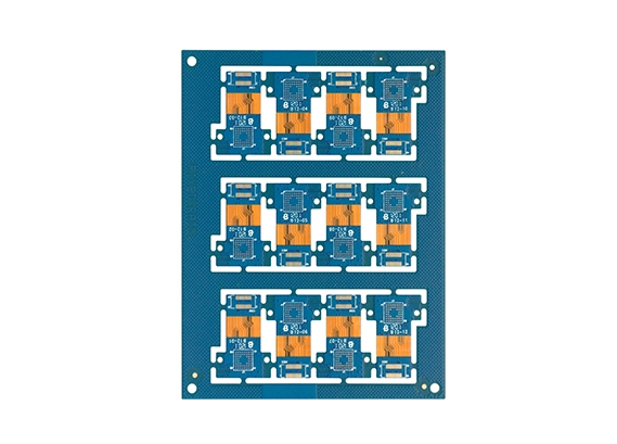
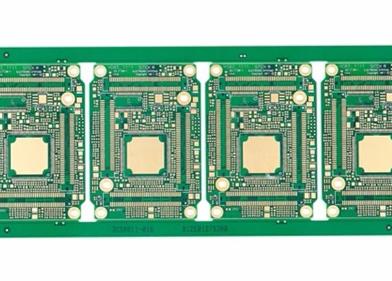
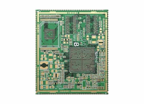
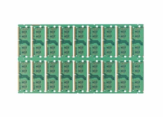
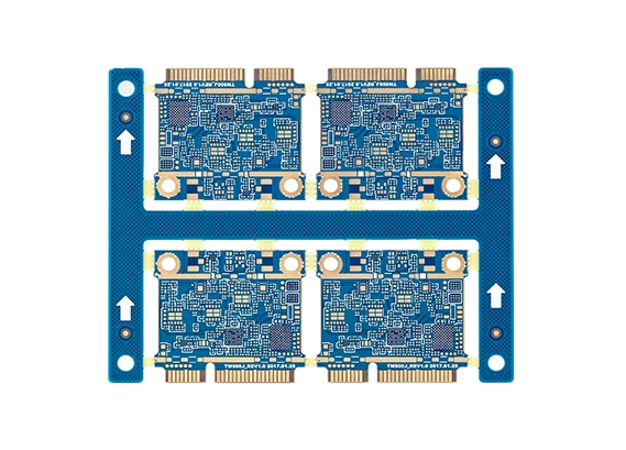
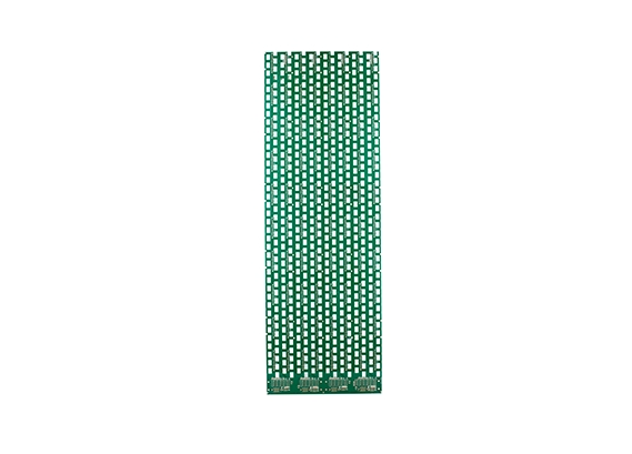
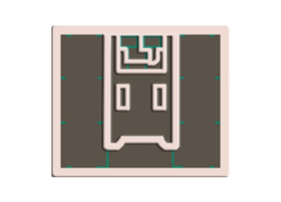
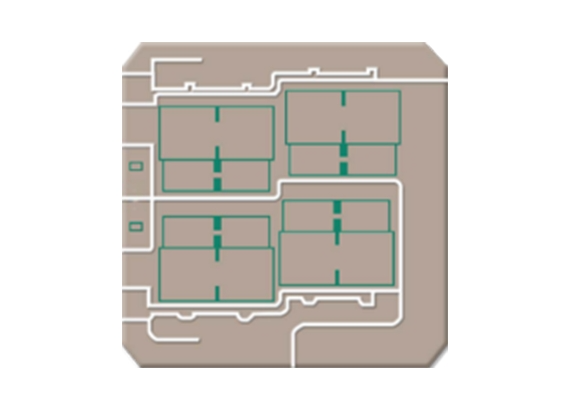
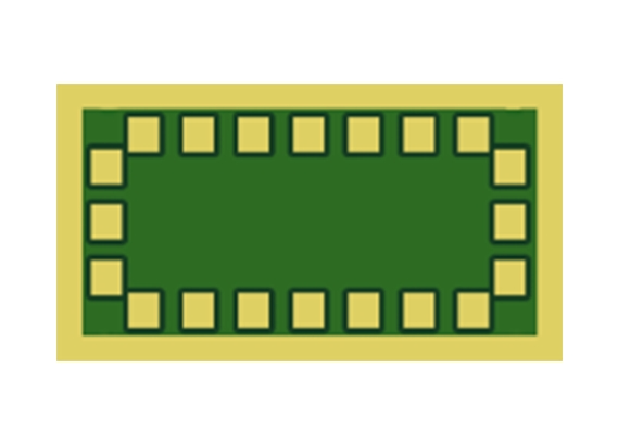
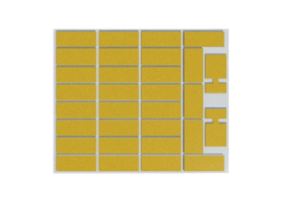
Automotive PCB
Number of Layers: 3L
Board Thickness: 6.5mm
Minimum Hole Diameter: 1.5mm
Minimum Line Width/Spacing: 2.0mm Inner Layer Copper Thickness: 4.0mm Outer Layer Copper Thickness: 3OZ Surface Finish: Immersion Gold (ENIG) Minimum Distance from Hole to Line: /
Board Thickness: 6.5mm
Minimum Hole Diameter: 1.5mm
Minimum Line Width/Spacing: 2.0mm Inner Layer Copper Thickness: 4.0mm Outer Layer Copper Thickness: 3OZ Surface Finish: Immersion Gold (ENIG) Minimum Distance from Hole to Line: /
Number of Layers: 6L
Board Thickness: 1.6mm
Minimum Hole Diameter: 0.1mm
Minimum Line Width/Spacing: 0.1mm/0.1mmInner Layer Copper Thickness: 18μm
Outer Layer Copper Thickness: 28μm
Surface Finish: Immersion Gold (ENIG)
Minimum Distance from Hole to Line: 0.15mm
Board Thickness: 1.6mm
Minimum Hole Diameter: 0.1mm
Minimum Line Width/Spacing: 0.1mm/0.1mmInner Layer Copper Thickness: 18μm
Outer Layer Copper Thickness: 28μm
Surface Finish: Immersion Gold (ENIG)
Minimum Distance from Hole to Line: 0.15mm
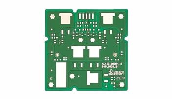
Number of Layers: L2
Board Thickness: 1.6mm
Minimum Hole Diameter: 0.8mm
Minimum Line Width/Spacing: 0.25/0.25mm
Inner Layer Copper Thickness: /
Outer Layer Copper Thickness: Localized 5-10μm
Surface Finish: Gold Plating (ENIG)
Minimum Distance from Hole to Line: /
Board Thickness: 1.6mm
Minimum Hole Diameter: 0.8mm
Minimum Line Width/Spacing: 0.25/0.25mm
Inner Layer Copper Thickness: /
Outer Layer Copper Thickness: Localized 5-10μm
Surface Finish: Gold Plating (ENIG)
Minimum Distance from Hole to Line: /
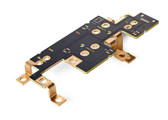
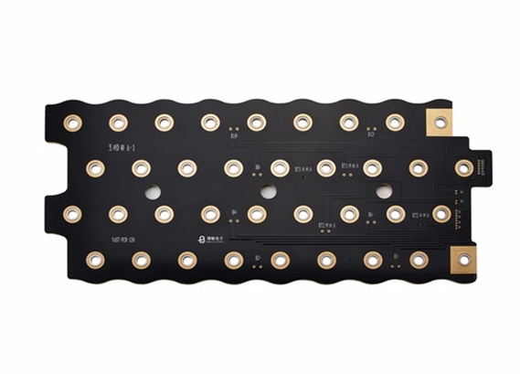
Number of Layers: 4L
Board Thickness: 5.0mm
Minimum Hole Diameter: 1.0mm
Minimum Line Width/Spacing: 0.5/0.27mm
Inner Layer Copper Thickness: 3.0mm
Outer Layer Copper Thickness: 1 OZ
Surface Finish: Immersion Gold (ENIG)
Minimum Distance from Hole to Line: Controlled Depth Milling + Bending
Board Thickness: 5.0mm
Minimum Hole Diameter: 1.0mm
Minimum Line Width/Spacing: 0.5/0.27mm
Inner Layer Copper Thickness: 3.0mm
Outer Layer Copper Thickness: 1 OZ
Surface Finish: Immersion Gold (ENIG)
Minimum Distance from Hole to Line: Controlled Depth Milling + Bending
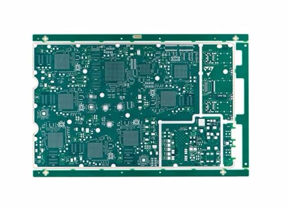
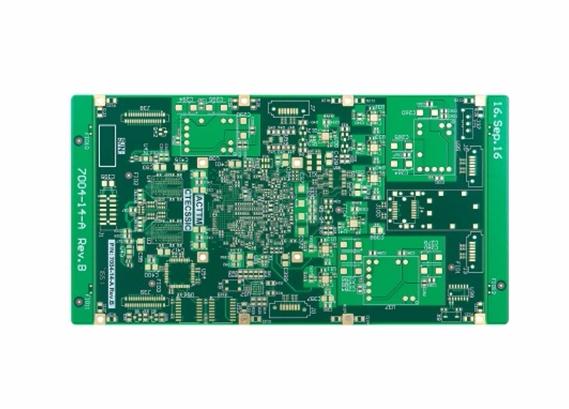
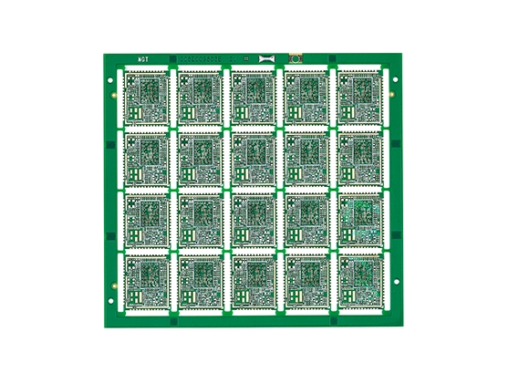
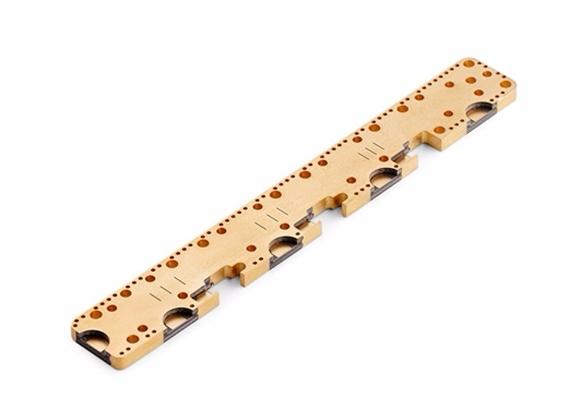
Industrial Control PCB
Number of Layers: 36L
Plate thickness: 8.0±0.8mm
Minimum aperture: 0.525mm
Minimum line width/line spacing: 0.0762/0.2388mm
Inner layer copper thickness: 2/1 OZ
Outer layer copper thickness: 53-73μm
Surface Treatment: Gold Plating ENIG
Minimum distance from hole to line: 0.2mm
Number of Layers: 1L + aluminum base
Plate thickness: 2.0mm
Minimum Hole Diameter:/
Minimum line width/line spacing: 0.3mm
Inner Layer Copper Thickness: /
Outer layer copper thickness: 4OZ
Surface Treatment: Hot Air Solder Leveling (HASL)
Minimum distance from point to line::/
Number of Layers: 4L
Plate thickness: 4.0mm
Minimum aperture: 0.65mm
Minimum Line Width/Line Spacing:/
Inner layer copper thickness: 4OZ
Outer layer copper thickness: 4OZ
Surface Treatment: Gold Plating ENIG
Minimum distance from point to line: /
Number of Layers: 14L
Plate thickness: 2.0±0.2mm
Minimum aperture: 0.275mm
Minimum line width/line spacing 0.1/0.125±20%
Inner Layer Copper Thickness: H/HOZ 1/1OZ
Outer layer copper thickness: 33-53μm
Surface Treatment: Immersion Tin
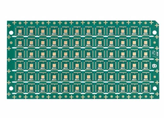
Consumer-related-PCB
Number of Layers: 4th to 6th floor
Plate thickness: 0.3-0.4mm
Minimum aperture: 0.075mm
Minimum line width/line spacing: 0.05mm
Inner layer copper thickness: 0.012mm
Outer layer copper thickness 0.025mm
Surface Treatment: Electroless Nickel Palladium Gold (ENEPIG)
Minimum distance from hole to line: 0.1mm
Number of Layers:2L
Plate thickness: 0.12mm
Minimum aperture: 0.1mm
Minimum line width/line spacing: 0.05mm
Inner layer copper thickness: 0.012mm
Outer layer copper thickness: 0.02mm
Surface Treatment: Gold Plating ENIG
Minimum distance from hole to line: 0.1mm
Number of Layers: 2L
Plate thickness: 0.12mm
Minimum aperture: 0.1mm
Minimum line width/line spacing: 0.05mm
Inner layer copper thickness: 0.012mm
Outer layer copper thickness: 0.02mm
Surface Treatment: Gold Plating ENIG
Minimum distance from hole to line: 0.1mm
Number of Layers: 8L
Plate thickness: 1.45mm
Minimum aperture: 0.25mm
Minimum line width/line spacing: 5/3.6 mil
Inner layer copper thickness: HOZ
Outer layer copper thickness: 1OZ
Surface Treatment: Gold Plating ENIG
Minimum distance from hole to line: 0.25mm
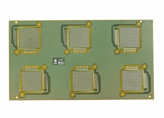
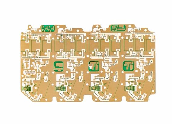
Medical device-PCB
Number of Layers: 12L
Plate thickness: 1.6mm
Minimum Aperture:0.45mm
Minimum line width/line spacing:0.09mm/0.1mm
Inner layer copper thickness:18μm
Outer layer copper thickness:25μm
Surface treatment: Immersion Gold ENIG
Minimum distance from point to line:0.18mm
Number of Layers: 14L
Plate thickness: 2.0mm
Minimum aperture: 0.25mm
Minimum line width/line spacing: 0.1mm/0.1mm
Inner layer copper thickness:18μm
外层铜厚:35μm
Surface treatment: Immersion Gold ENIG
Minimum distance from hole to line: 0.2mm
Number of Layers: 8L
Plate thickness: 0.8mm
Minimum aperture: 0.2mm
Minimum line width/spacing: 3.5/3 mil
Inner Layer Copper Thickness: HOZ
Outer layer copper thickness: 1OZ
Surface Treatment: Gold Plating ENIG
Minimum distance from hole to line: 0.18mm
Number of Layers: 16L
Plate thickness: 2.0mm
Minimum aperture: 0.2mm
Minimum line width/line spacing: 0.08mm
Inner Layer Copper Thickness: HOZ
Outer layer copper thickness: 1OZ
Surface Treatment: Gold Plating ENIG
Minimum distance from hole to line: 0.16mm
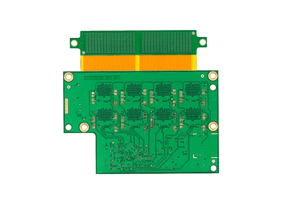
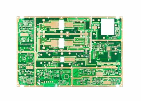
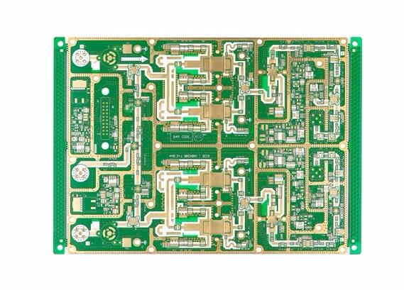
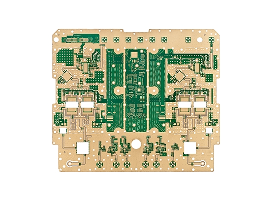
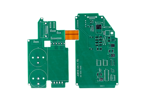
Communication -PCB
Number of Layers: 8L
Plate thickness: 1.20mm
Minimum aperture: 0.25mm
Minimum line width/line spacing: 0.081/0.127mm
Inner layer copper thickness: H/H
Outer layer copper thickness: 15-33μm
Surface Treatment: Gold Plating ENIG+OSP
Minimum distance from point to line:/
Number of floors: 6L (1+4BV+1)
Plate thickness: 0.6mm
Minimum aperture: 0.1mm
Minimum line width/line spacing: 0.075mm/0.075mm
Inner layer copper thickness: 18μm
Outer layer copper thickness: 28μm
Surface Treatment: Gold Plating ENIG
Minimum distance from hole to line: 0.18mm
Number of Layers: 4L
Plate thickness: 1.0mm
Minimum aperture: 0.2mm
Minimum line width/line spacing: 0.127mm
Inner layer copper thickness: 1 oz
Outer layer copper thickness: 1.5OZ
Surface Treatment: Gold Plating ENIG
Minimum distance from hole to line: 0.2mm
Number of Layers: 28L
Plate thickness: 6.5mm
Minimum aperture: 0.7 millimeters
Minimum line width/line spacing: 0.1mm
Inner layer copper thickness: 1 oz
Outer Layer Copper Thickness: TOZ+
Surface Treatment: Gold Plating ENIG
Minimum distance from hole to line: 0.18mm
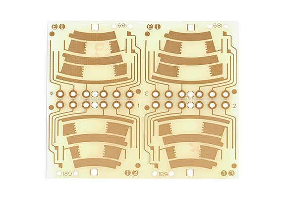
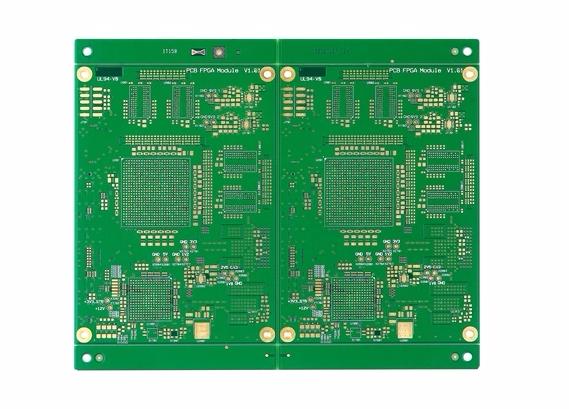
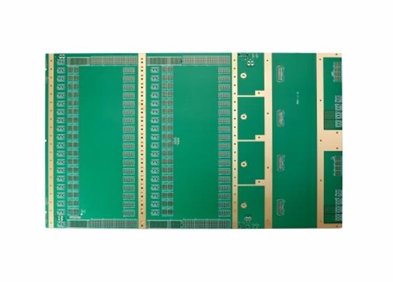
High-frequency microwave-PCB
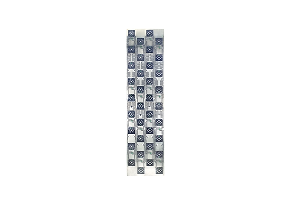
Number of Layers:2L
Plate thickness: 0.6mm
Minimum aperture: 0.8mm
Minimum line width/line spacing: 0.12mm
Inner Layer Copper Thickness: /
Outer layer copper thickness: 1OZ
Surface Treatment: Immersion Tin
Minimum distance from point to line:/
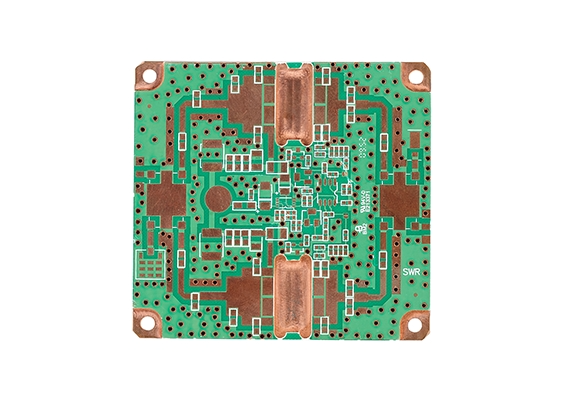
Number of layers: 4L + copper base
Plate thickness: 5.6mm
Minimum aperture: 0.35mm
Minimum line width/spacing: 1.25mm
Inner Layer Copper Thickness: HOZ
Outer layer copper thickness: 1OZ
Surface Treatment: Gold Plating ENIG
Minimum distance from hole to line: 0.185mm
Number of Layers: 6
Plate thickness: 3.0mm
Minimum aperture: 0.3mm
Minimum line width/line spacing: 0.25mm
Inner layer copper thickness: 1 oz
Outer layer copper thickness: 1OZ + Plating
Surface Treatment: Gold Plating ENIG
Minimum distance from hole to line: 0.2mm
Number of Layers: 4L
Plate thickness: 2.0mm
Minimum aperture: 0.3mm
Minimum line width/line spacing: 0.175mm
Inner layer copper thickness: HOZ
Outer layer copper thickness: 1OZ
Surface Treatment: Gold Plating ENIG
Minimum distance from hole to line: 0.18mm
Communication -PCB
Number of Layers: 6
Plate thickness: 1.6mm
Minimum aperture: 0.2mm
Minimum line width/line spacing: 0.075mm/0.075mm
内层铜厚: 35μm
外层铜厚: 35μm
表面处理: 化金 ENIG
孔到线最小距离:0.16mm
层数:10L
Plate thickness: 1.0mm
Minimum aperture: 0.1mm
Minimum line width/line spacing: 0.075mm/0.075mm
内层铜厚: 35μm
外层铜厚: 35μm
表面处理: 化金+金手指+斜边ENIG+OSP+Beveling of G/F
孔到线最小距离:0.16mm
层数:4L
板厚:0.3±0.05mm
最小孔径:0.3mm
最小线宽/线距:0.0508/0.084mm
内层铜厚: H/HOZ
外层铜厚: 17-23μm
表面处理: 化学镍钯金 ENEPIG
孔到线最小距离: 0.2mm
层数:6L
板厚:0.3±0.05mm
最小孔径:0.6mm
最小线宽/线距:0.05/0.05mm
内层铜厚: T/TOZ
外层铜厚: 15-33μm
表面处理: 化金 ENIG
孔到线最小距离: 0.2mm
层数:8L
板厚:3.2mm
最小孔径:0.4mm
最小线宽/线距:0.25/0.25mm
Inner layer copper thickness: 1 oz
外层铜厚: 2OZ
表面处理: OSP
孔到线最小距离: 抗氧化 OSP
层数:4L
板厚:4.8mm
最小孔径:0.5mm
最小线宽/线距:0.15mm
内层铜厚: LOZ
外层铜厚: LOZ+plating
Surface Treatment: Gold Plating ENIG
孔到线最小距离:0.35mm
层数:6L
板厚:1.1mm
最小孔径:0.3mm
最小线宽/线距:0.15mm
内层铜厚:LOZ
外层铜厚:HOZ+plating
表面处理:电镀金 Gold Plating
孔到线最小距离:0.25mm
层数:8L
板厚:硬板 1.95-2.35mm FPC0.66±0.06mm
最小孔径:0.6mm
最小线宽/线距:0.122mm
内层铜厚: H/HOZ
外层铜厚: 45-60μm
表面处理: 喷锡 HASL
孔到线最小距离: 0.38mm
Other Product Solutions
产品:IGBT载板
基材材质:氮化硅
基材材质:氮化硅
基材厚度:0.32mm
最小线宽/线距:0.50mm/0.50mm
表面处理:OSP
应用领域:高电压、大电流、功率模块、
IGBT
IGBT
特殊工艺:无空洞钎焊,厚铜精准蚀刻
产品:IGBT载板
基材材质:氧化铝
基材材质:氧化铝
基材厚度:0.635mm
最小线宽/线距:0.40mm/0.40mm
表面处理:OSP
应用领域:高电压、大电流、功率模块、
IGBT
IGBT
特殊工艺:厚铜精准蚀刻
产品:功率模块载板
基材材质:99.6%氧化铝
基材材质:99.6%氧化铝
基材厚度:0.5mm
最小线宽/线距:0.10mm/0.10mm
表面处理:正面:Ni/Au≥4μm;背面:Ni/Au≥0.5μm;
应用领域:航空航天、武器装备
特殊工艺:Φ0.2mm通孔填孔,面铜5±1μm,Rz≤2μm
产品:陶瓷基板(TEC)
基材材质:氧化铝
基材厚度:0.5mm
Minimum Line Width/Line Spacing:/
表面处理:化学镍钯金
应用领域:TEC致冷片
特殊工艺:/
产品:LD热沉(COS)
基材材质:氮化铝
基材厚度:0.34mm
Minimum Line Width/Line Spacing:/
表面处理:电镀镍金
应用领域:LD半导体激光COS封装
特殊工艺:预制金锡共晶

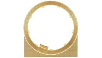
产品:微带环形器
基材材质:铁氧体
基材材质:铁氧体
基材厚度:0.5mm
最小线宽/线距:0.10mm/0.10mm
表面处理:电镀纯金
应用领域:微带环形器
特殊工艺:多种金属混合溅射,25μm金丝拉力≥9g

产品:微带隔离器
基材材质:铁氧体
基材厚度:0.4mm
最小线宽/线距:0.10mm/0.10mm
表面处理:Cu≥4μm,Au≥2.5μm
应用领域:微带隔离器
特殊工艺:金线路精准蚀刻,TaN隔离电阻,阻值40-50Ω精准控制

产品:薄膜电容
基材材质:氮化铝
基材厚度:0.4mm
最小线宽/线距:0.15±0.005mm/0.07±0.005mm
表面处理:正面:Au≥1.0μm;背面:Au≥0.5μm;
应用领域:电容器
特殊工艺:最小线宽30μm,精准蚀刻厚金